- 您现在的位置:买卖IC网 > Sheet目录1993 > DS1083LR-U+ (Maxim Integrated Products)IC CLOCK MOD SS 3.3V TSOT23-6
ABSOLUTE MAXIMUM RATINGS
RECOMMENDED OPERATING CONDITIONS
(TA = -40°C to +125°C, unless otherwise noted.)
Stresses beyond those listed under “Absolute Maximum Ratings” may cause permanent damage to the device. These are stress ratings only, and functional
operation of the device at these or any other conditions beyond those indicated in the operational sections of the specifications is not implied. Exposure to
absolute maximum rating conditions for extended periods may affect device reliability.
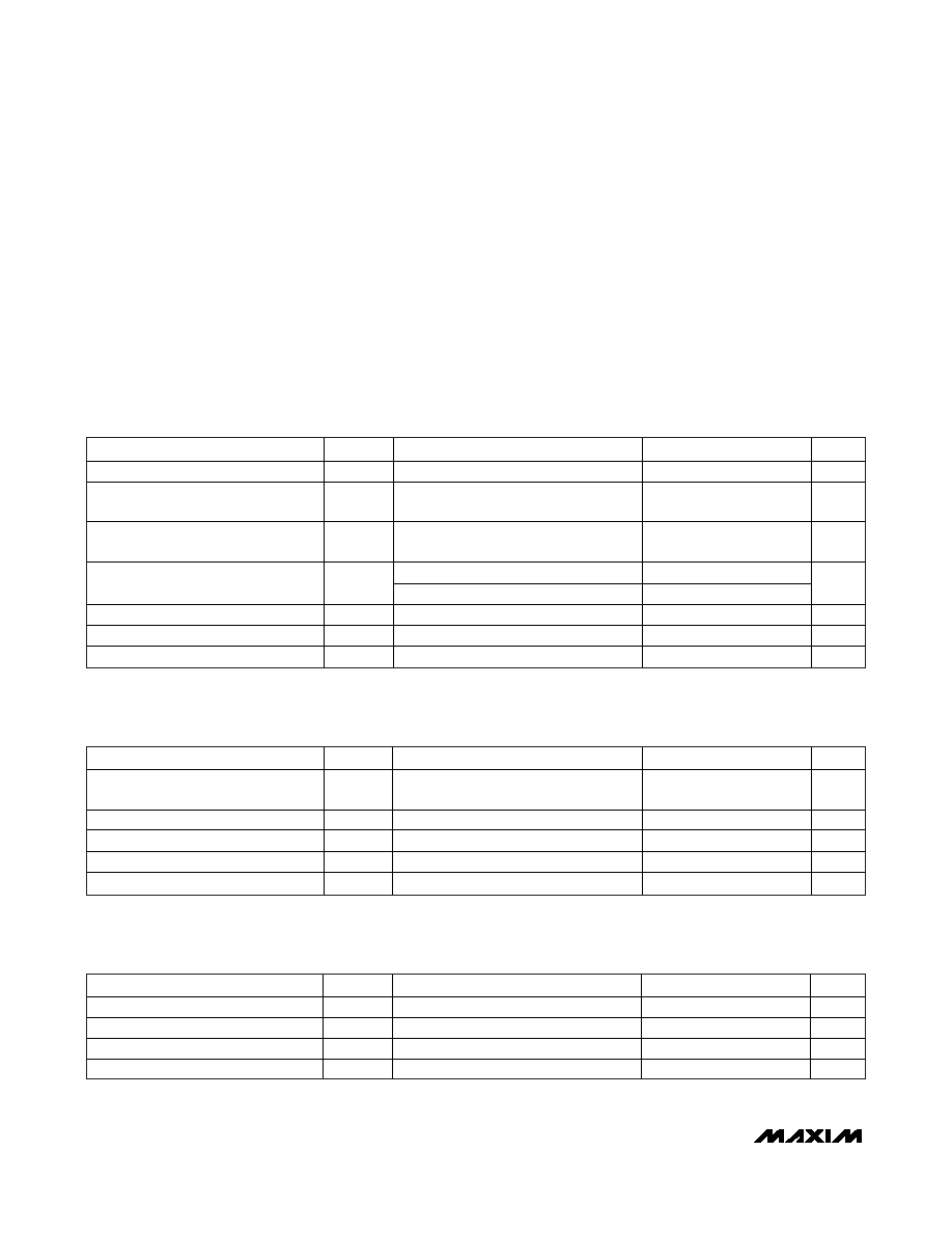
Voltage Range on VCC Relative to GND.............-0.5V to +3.63V
Voltage Range on Any Lead Relative
to GND ................-0.5V to (VCC + 0.5V), not to exceed +3.63V
Operating Temperature Range .........................-40°C to +125°C
Storage Temperature Range .............................-55°C to +125°C
Soldering Temperature...........................Refer to the IPC/JEDEC
J-STD-020 Specification.
PARAMETER
SYMBOL
CONDITIONS
MIN
TYP
MAX
UNITS
VCC Supply Voltage
VCC
(Note 1)
3.0
3.6
V
SMSEL1/SMSEL2 Input Logic 1
VIH
0.7 x
VCC
VCC +
0.3
V
SMSEL1/SMSEL2 Input Logic 0
VIL
-0.3
0.3 x
VCC
V
fSSO < 80MHz
15
SSO Load
CL
80MHz
fSSO < 134MHz
7
pF
CLKIN Frequency
fIN
16
134
MHz
CLKIN Duty Cycle
fINDC
40
60
%
VCC Power-Up Time
tPV
GND to VCCMIN
200
ms
DC ELECTRICAL CHARACTERISTICS
(VCC = +3.0V to +3.6V, TA = -40°C to +125°C, unless otherwise noted.)
PARAMETER
SYMBOL
CONDITIONS
MIN
TYP
MAX
UNITS
Supply Current
ICC
CL = 7pF,
fIN = 134MHz
15
mA
SMSEL1/SMSEL2 Pullup Resistance
RPU
TA = +25°C
60
100
140
k
SMSEL1/SMSEL2 Input Leakage
IIL
0V < VIN < VCC
±80
μA
Low-Level Output Voltage (SSO)
VOL
IOL = 4mA
0.4
V
High-Level Output Voltage (SSO)
VOH
IOH = -4mA
2.4
V
AC ELECTRICAL CHARACTERISTICS
(VCC = +3.0V to +3.6V, TA = -40°C to +125°C, unless otherwise noted.)
PARAMETER
SYMBOL
CONDITIONS
MIN
TYP
MAX
UNITS
SSO Duty Cycle
fSSODC
Measured at VCC/2
40
60
%
SSO Rise Time
tR
CL = 7pF
1
ns
SSO Fall Time
tF
CL = 7pF
1
ns
Peak Cycle-to-Cycle Jitter
tJ
TA = -40°C to +85°C, 10,000 cycles
75
ps
DS1083L
16MHz to 134MHz Spread-Spectrum
Clock Modulator for LCD Panels
2
_______________________________________________________________________________________
Note 1: All voltages referenced to ground. Currents into the IC are positive and currents out of the IC are negative.
发布紧急采购,3分钟左右您将得到回复。
相关PDF资料
DS1100LZ-75+W
IC DELAY LINE 5TAP 75NS 8-SOIC
DS1100M-75+
IC DELAY LINE 5TAP 75NS 8-DIP
DS1110LE-125+
IC DELAY LINE 10TAP 14-TSSOP
DS1110S-80+
IC DELAY LINE 10TAP 16-SOIC
DS1123LE-100+
IC DELAY LINE 256TAP 16-TSSOP
DS1124U-25+T
IC DELAY LINE 256TAP 10-USOP
DS1135LU-300/T&R
IC DELAY LINE 300NS 8-USOP
DS1135Z-12/T&R
IC DELAY LINE 12NS 8-SOIC
相关代理商/技术参数
DS1085
制造商:DALLAS 制造商全称:Dallas Semiconductor 功能描述:EconOscillator Frequency Synthesizer
DS1085L
制造商:MAXIM 制造商全称:Maxim Integrated Products 功能描述:3.3V EconOscillator Frequency Synthesizer
DS1085LZ-12
功能描述:可编程振荡器 3.3V EconOscillator f Synthesizer RoHS:否 制造商:IDT 封装 / 箱体:5 mm x 7 mm x 1.5 mm 频率:15.476 MHz to 866.67, 975 MHz to 1300 MHz 频率稳定性:+/- 50 PPM 电源电压:3.63 V 负载电容:10 pF 端接类型:SMD/SMT 输出格式:LVPECL 最小工作温度:- 40 C 最大工作温度:+ 85 C 尺寸:7 mm W x 5 mm L x 1.5 mm H 封装:
DS1085LZ-12+
功能描述:可编程振荡器 3.3V EconOscillator f Synthesizer RoHS:否 制造商:IDT 封装 / 箱体:5 mm x 7 mm x 1.5 mm 频率:15.476 MHz to 866.67, 975 MHz to 1300 MHz 频率稳定性:+/- 50 PPM 电源电压:3.63 V 负载电容:10 pF 端接类型:SMD/SMT 输出格式:LVPECL 最小工作温度:- 40 C 最大工作温度:+ 85 C 尺寸:7 mm W x 5 mm L x 1.5 mm H 封装:
DS1085LZ-12B2
功能描述:可编程振荡器 RoHS:否 制造商:IDT 封装 / 箱体:5 mm x 7 mm x 1.5 mm 频率:15.476 MHz to 866.67, 975 MHz to 1300 MHz 频率稳定性:+/- 50 PPM 电源电压:3.63 V 负载电容:10 pF 端接类型:SMD/SMT 输出格式:LVPECL 最小工作温度:- 40 C 最大工作温度:+ 85 C 尺寸:7 mm W x 5 mm L x 1.5 mm H 封装:
DS1085LZ-12B2+
功能描述:可编程振荡器 3.3V EconOscillator f Synthesizer RoHS:否 制造商:IDT 封装 / 箱体:5 mm x 7 mm x 1.5 mm 频率:15.476 MHz to 866.67, 975 MHz to 1300 MHz 频率稳定性:+/- 50 PPM 电源电压:3.63 V 负载电容:10 pF 端接类型:SMD/SMT 输出格式:LVPECL 最小工作温度:- 40 C 最大工作温度:+ 85 C 尺寸:7 mm W x 5 mm L x 1.5 mm H 封装:
DS1085LZ-25
功能描述:可编程振荡器 3.3V EconOscillator f Synthesizer RoHS:否 制造商:IDT 封装 / 箱体:5 mm x 7 mm x 1.5 mm 频率:15.476 MHz to 866.67, 975 MHz to 1300 MHz 频率稳定性:+/- 50 PPM 电源电压:3.63 V 负载电容:10 pF 端接类型:SMD/SMT 输出格式:LVPECL 最小工作温度:- 40 C 最大工作温度:+ 85 C 尺寸:7 mm W x 5 mm L x 1.5 mm H 封装:
DS1085LZ-25+
功能描述:可编程振荡器 3.3V EconOscillator f Synthesizer RoHS:否 制造商:IDT 封装 / 箱体:5 mm x 7 mm x 1.5 mm 频率:15.476 MHz to 866.67, 975 MHz to 1300 MHz 频率稳定性:+/- 50 PPM 电源电压:3.63 V 负载电容:10 pF 端接类型:SMD/SMT 输出格式:LVPECL 最小工作温度:- 40 C 最大工作温度:+ 85 C 尺寸:7 mm W x 5 mm L x 1.5 mm H 封装: